
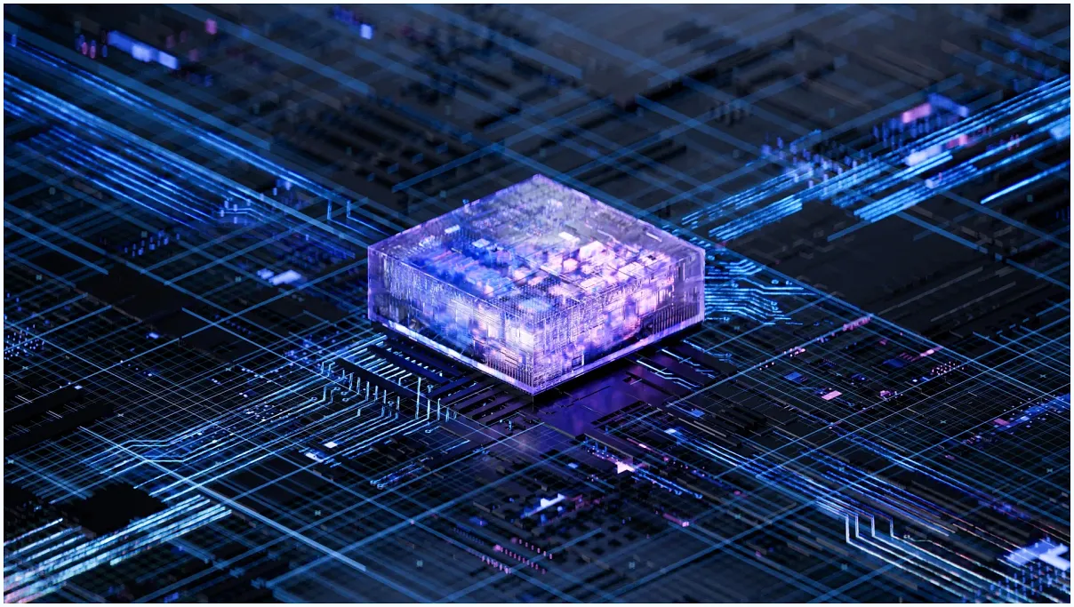
For decades, the gospel of computing has been clear: smaller, faster. Pack more transistors onto a chip. Moore's Law, they called it. An era-defining trajectory. But physics, alas, has a way of reminding us of its limits.
Those microscopic components? They're bumping up against atomic scales. Silicon, once the limitless playground, is starting to show its age. Quantum mechanics. It’s no longer just about shrinking.
What if the answer isn't smaller, but up?
A team at the University of Illinois Grainger College of Engineering, led by materials science and engineering professor Qing Cao, thinks they’ve cracked it. They’ve demonstrated a radical new method: stacking multiple layers of silicon electronics, one directly on top of the other. Not just theoretical. This could be the breakthrough the industry has been waiting for. More power. Less energy. A lifeline for computing's relentless pace.
Imagine your computer's brain. Now imagine it as a sprawling suburban landscape. Cao's vision? High-rises. "Take something as simple as static random-access memory, which is universal in CPUs and GPUs," Cao explained. "Today it takes six microelectronic devices called transistors on a single plane to store one bit of information. With vertical integration, you can distribute them across multiple layers. It's like replacing a sprawling suburb with high-rises: you get the same functionality, but the spatial footprint is reduced while making communication between layers faster and more efficient."
This isn't just a lab curiosity. Their process boasts device yields of 98-100%. Using standard single-crystalline silicon. That means it’s not some exotic material. It could actually be adopted by commercial chip manufacturers. Soon.
Sure, vertical integration already exists in some AI hardware. But that's usually about bonding separate, finished wafers. Monolithic integration is the holy grail. Fabricating each layer directly on the last. Denser connections. Nanometer-level alignment. A game-changer.
The Heat is On: Conquering Silicon's Oldest Foe
The biggest hurdle? Heat. Producing quality crystalline silicon demands temperatures pushing 1,000 degrees Celsius. Utterly destructive to existing metal interconnects in a completed circuit layer. Industry accepted a hard limit: 400 degrees Celsius for any subsequent layers. Most researchers gave up on pure silicon for the upper layers, opting for compromise materials. Always a performance hit. Always reliability issues.
"For the first time, we have met the thermal budget of monolithic 3D integration using standard single-crystalline silicon and delivered unprecedented performance."
Cao's team didn't compromise. They found a way. Ultrathin freestanding silicon nanomembranes. They create these wafer-thin films, then transfer them onto an existing circuit using a roll laminator. The magic? This bonding needs only 200 degrees Celsius. Well below the danger zone. The silicon retains its crystalline quality. Performance? Unaffected. Reliability? Intact.
These membranes are astonishingly thin. Just 10 nanometers. A human hair is 50,000 to 100,000 nanometers. They conform perfectly to the underlying surface, avoiding those pesky defects that plague traditional wafer bonding. Ingenious.
They even redesigned the transistor. Traditional doping needs high heat. So they used "junctionless transistors." Heavily doped silicon before stacking. The thin films allow precise control. Low parasitic resistance. A clever workaround.
The result? Three stacked layers. 625 transistors each. Uniformity. High yield. Current densities matching conventional silicon transistors made at vastly higher temperatures. Outperforming alternatives by a factor of three or four. They even built 3D logic circuits and static random-access memory cells. Fully functional.
Scalability. That's the real headline, Cao insists. More layers are possible. High-performing transistors, reliable. Low variability. The foundation is laid. For industrial foundries. For commercial production.
The era of 3D silicon chips? It's not just a distant dream anymore. It's here. Ready to reshape what we thought possible in computing. The next chapter has begun. And it’s built upwards.



No comments yet. Be the first to share your thoughts!